How can electrons be “topological”?
The following text is an excerpt from a draft of an article that I co-wrote for the magazine Physics Today, together with Prof. Art Ramirez at UC Santa Cruz. The article will appear (edited, and with more professional figures) in the magazine in September. The article attempts to give some intuition about the concept of “topological” electron bands, which have become very important in modern condensed matter physics.
Dawn of the Topological Age?
Historians often label epochs of human history according to their material technologies. For example, we have the bronze age, the iron age and, more recently, the silicon age. From the physicist’s perspective, the silicon age began with the interplay of theory, experiment, and device prototyping of a new type of material, the semiconductor. Semiconductors had been known since the late 1800s as materials with unusual sensitivity to light, to the method of synthesis, and to the direction of current flow. It was not until the early 1930s, however, that a theoretical understanding of semiconductors approached its modern form [1]. The prevailing view at the time saw metals and insulators as opposite limits of electron itineracy, adiabatically controlled by the probability for an electron to hop between atoms. But the recently-developed idea of accessible electron energies (bands) and inaccessible energies (band gaps) provided a natural category for semiconductors – they were more like insulators, but with smaller band gaps, often controlled by impurities. The next fifteen years witnessed breakthroughs in the purification and control of dopants in the elemental semiconductors silicon and germanium that eventually enabled the discovery of transistor action at Bell Labs in 1947. A surprise came during the transistor patent preparation, however. The basic idea underlying the field effect transistor had already been patented in 1930 by Julius Lillienfeld, an Austrian-Hungarian physicist who had emigrated the United States in 1921.
For semiconductors, the path from materials discovery to device implementation was neither linear nor easily predicted. For a relatively new class of materials, called “topological” materials, one can notice compelling analogies with the development of semiconductors, suggesting the tantalizing possibility that we are at the dawn of the “topological age”. In this article, we will describe what it means for materials to be “topological,” and why topology raises the prospect for revolutionary new devices.
The “shape” of an electron band
The notion of a topological invariant comes from a branch of mathematics called topology, which studies properties of geometric objects that are conserved under continuous deformations. The most famous such property is the genus, g, which is an integer that counts the number of holes in a three-dimensional (3D) shape (i.e., g = 0 for a sphere or a plate, g = 1 for a donut or a coffee mug, g = 3 for a pretzel, etc.). The genus is defined via the Gauss-Bonnet theorem, which states that the integral of Gaussian curvature K over the surface S of an object is quantized:

Here 


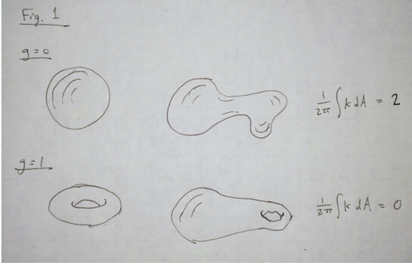
Fig. 1 A topological invariant is a property of a geometric shape that does not change when the shape is stretched or distorted. One such invariant is the genus g, which is defined by the number of holes in the surface and is related to the integral of the Gaussian curvature K over the surface of the shape. For example, shapes with no holes in them (g = 0) all give the same value of this integral, as do shapes with one hole in them (g = 1).
Much of the recent excitement surrounding “topological electronics” originates in the prospect of finding physical properties of electronic systems that behave like this integer-valued genus. Such an invariant property is necessarily robust to small perturbations or defects, since integers cannot change continuously. In the remainder of this section we will explain the origin of a commonly-discussed invariant, the Chern number, which is what defines a “topological electron band”.
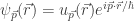
Within a single isolated atom, electrons occupy discrete quantum energy levels, or orbitals. When many atoms are arranged into a crystal, the wave functions from neighboring atoms hybridize with each other, and the orbitals broaden into bands of states having a range of energies. Each of the states within a band describes an electron that is shared among many atoms, and its wave function can be written in terms of the momentum 
The factor 

Importantly, the electron momentum 
Constructing an analogy with the Gauss-Bonnet theorem for electron bands requires an analog of the “curvature” that is integrated over a closed surface. As it turns out, this analog of curvature arises from the properties of the Bloch functions 


This quantity 


Fig. 2 Inside a crystal, the “free particle” electron states are described by a slowly-oscillating plane wave (blue curve) that is modulated by Bloch functions (black curve), which describe the electron’s attraction to the atoms (red and blue circles) within the repeating unit cell of the crystal. For a given momentum state, the electron probability density (shaded black areas on the left) is shared among the atoms within the unit cell in way that can depend on the momentum
Imagine now the hypothetical process of accelerating and then decelerating an electron in such a way that the electron returns to its initial momentum. During the course of this cyclic process the electron traces out a path 

(This expression for the phase is analogous to how a particle traversing a path in position space experiences a phase shift 


Fig. 3 The set of all possible momenta p for electrons within the crystal defines a Brillouin zone (denoted BZ, and illustrated for a 2D system by the black square). Opposite edges of the BZ describe the same wave function, and therefore are equivalent to each other. The Berry connection 
The Berry phase becomes particularly instructive if we consider how it behaves for paths on a closed two-dimensional (2D) surface of momenta. For example, the Brillouin zone of a 2D system effectively acts like a closed surface because opposite edges of the zone are equivalent to each other. Consider, in particular, the path shown in Fig. 3, which traverses the Brillouin zone boundary of a 2D system. Traversing this path in the clockwise direction yields some Berry phase 


where 

One can notice that, even though local symmetries do not define the Chern number, having 


Below we discuss this idea and other implications of electron topology, as well as its generalization to 3D systems.
Implications of Topology
One can notice from Fig. 3 that a nonzero Chern number implies a “winding” or “self-rotation” in the structure of the electron wave function. This self-rotation is associated with a physical angular momentum for electrons. For example, if one imagines making a wave packet using states from some particular region of momentum space, one sees that there is a relation between the position (within the unit cell) and the momentum of the states that comprise the wave packet. This relation between position and momentum implies an angular momentum for the wave packet that depends on the local Berry curvature. In this sense the Berry curvature is again like a magnetic field, created by a broken symmetry in the material itself rather than by any external source, in that it gives electrons an angular momentum.
The analogy of Berry curvature to magnetic field can be made more precise by considering the effects of an applied electric field 


In this way, the anomalous velocity is like the E-cross-B drift experienced by an electron in crossed electric and magnetic fields. Applying an electric field in a particular direction causes an electron to drift in a direction that is, in part, transverse to both the field and the direction of the (momentum-dependent) Berry curvature, which acts like a magnetic field.
One of the most striking implications of the magnetic field analogy arises from the motion of electrons at the boundary of a sample. In a conductor with no intrinsic Berry phase that is subjected to a magnetic field, electrons near the boundary perform “skipping orbits”, essentially rolling along the boundary in a direction that is defined by the magnetic field direction. No matter how the boundary is shaped, these skipping orbits persist, providing a single conducting channel for current to flow through. In a similar way, the self-rotation implied by a finite Chern number guarantees the existence of traveling edge states. In 2D electron systems with a magnetic field (and sufficiently high electron mobility), the skipping orbit states give rise to the celebrated Quantum Hall Effect, including a quantized electrical conductance whose value is completely universal. 2D materials with finite Chern number have this same universal conductance, even though no magnetic field is present.
In fact, the existence of a topological invariant for electron systems subjected to a magnetic field was first identified by Thouless, Kohomoto, Nightingale and den Nijs (TKNN) [4]. This topological invariant allows for a remarkable universality of the quantum Hall effect among different samples and materials. In fact, the TKNN invariant allows the universal constant 

There is an important way, however, in which the edge states of a topological material can be different from the edge states of a quantum Hall system. In a quantum Hall system, the magnetic field breaks the time-reversal symmetry of the system, since the magnetic field forces electrons to turn in spiral trajectories with a particular handedness, clockwise or counterclockwise, that is set by the magnetic field direction. These spiral trajectories break time reversal symmetry since playing them backwards in time (without reversing the sign of the external magnetic field) produces motion that is inconsistent with the Lorentz force law.
But it is possible to have a topological electron band, and its associated edge states, even in a material that has time-reversal symmetry. The key idea is to combine broken inversion symmetry in the material with a strong coupling between the electron’s momentum and its spin. For example, in the simplest case of a quantum spin Hall insulator, these two ingredients combine to allow the two different electron spin states to have nonzero but opposite Chern number. To see how this possibility can arise, consider that the time reversal operation also reverses an electron’s spin, so that, under time reversal, a left-going-spin-up electron becomes a right-going-spin-down electron. Thus, a topological electron band can retain time-reversal symmetry if the bands for spin-up and spin-down electrons have opposite Chern number (Fig. 4). Opposite Chern number means that the two spin species have opposite-moving edge states. This locking of the direction of the edge state to the spin is called the quantum spin Hall effect, and it was discovered experimentally in 2007 following its experimental prediction in 2003.

Fig. 4. A quantum spin Hall system has equal and opposite Chern number for its two spin species. (a) The Berry connection 
Ultimately, the locking of spin to momentum at edge states arises from the microscopic spin-orbit, or “
Topological bands in three dimensions
So far we have only discussed one example of a topological invariant: the Chern number in a 2D band, which gives rise to edge states very much like those in the quantum Hall effect. But a range of 3D materials have been identified with electrical properties that are protected by a topological invariant. These include the 3D topological insulators, which are largely made from narrow band-gap semiconductors with strong spin-orbit coupling [6]. In these materials, an electrically insulating interior coexists with surface states that form 2D metals on every free surface and have a similar locking of the electron’s spin perpendicular to its momentum.
The 2D Chern number discussed above can also be applied to understand another class of 3D materials: the Weyl semimetals. These materials have special points in momentum space where their “topological charge” is concentrated. To see why this happens, imagine defining an arbitrary closed surface S of momentum states within the 3D Brillouin zone of some material (Fig. 5). One can apply to this surface the same arguments about Berry phase that we used for the 2D case, and arrive at the conclusion that the Chern number associated with the surface must also be quantized. In particular,
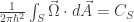
where, 

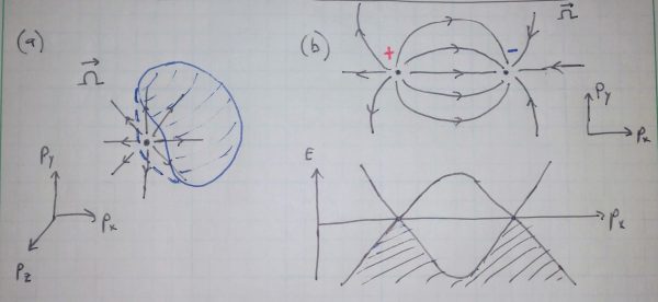
Fig. 5. A Weyl semimetal has monopole sources of Berry curvature and points where two different electron bands meet. (a) The Berry curvature 


From a materials perspective, Weyl points arise when strong spin-orbit coupling causes two bands of states with different angular momentum to coincide in energy. Since the orbital character of the wave function must change abruptly upon crossing from one band to another, Weyl points correspond to the locations in momentum space where the two bands touch. In the usual metals and semiconductors that comprise the majority of our electronic technologies, such touching of bands is unusual. Typically, electronic bands cannot coincide in energy because of the phenomenon of avoided crossing — the quantum phenomenon of hybridization of degenerate quantum states into symmetric and antisymmetric combinations that have different energies. However, it was recognized as early as 1937, in a paper by Conyers Herring that presaged much of modern topological band theory [7], that two electron bands could meet in energy because of “accidental degeneracies” that prevent the two bands from hybridizing. In these cases, a perturbation that removes an accidental degeneracy can destroy the band crossing point and open a gap. In Weyl semimetals, however, the Weyl points are protected by the quantization of the Chern number. Only a sufficiently strong perturbation, which effectively brings two oppositely-charged Weyl points together, can destroy the degeneracy and open a gap between two electron bands. Thus, a Weyl semimetal is a topologically-protected gapless system (a semimetal). Like the other topological materials, Weyl semimetals have intriguing surface states. In particular, the surfaces of Weyl semimetals exhibit Fermi arcs, or momentum states ranging from one Weyl point momentum to another [9].
Experimentally, the study of topological materials is progressing rapidly, with new compounds, even whole classes of topological materials, being discovered routinely. The initial discovery of 3D topological insulating behavior was made using angle-resolved photoemission spectroscopy (ARPES) in Bi1-xSbx, a mixture of two non-topological semimetals, each with spin orbit coupled bands, that produces a bulk semiconductor for 0.07 < x < 0.22 [12]. Since that discovery, many other topological insulators, as well as Weyl and nodal-line semimetals, have been identified. While ARPES remains a primary tool for revealing electronic band structures, the transport properties of topological materials are also being intensely studied, and raise the possibility of new device functionalities.
What technologies will topological materials enable?
The usefulness of many materials comes from their ability to either pass a current of some kind, or to prevent a current from flowing. For example, copper is useful because it allows electric current to flow freely down the length of a wire, while the polymer encasing the wire is useful because it blocks the current from leaking out. Other examples include materials for passing or blocking heat currents (like heat sinks on computer processors, or the insulating foam on the space shuttle) or filtering light (like the lenses on protective sunglasses, which pass some light frequencies while blocking others). Seen from this perspective, the “silicon age” arose because silicon can act as a kind of switchable valve, an “on/off switch” for electrical current. We know now that pure silicon is a good insulator, but if a “gate” voltage is applied to its surface it becomes an electrical conductor.
Thus, for developing new electronic materials, the main goals are usually filtering and sensitivity. The material should be able to selectively pass or block a generalized current (like silicon can selectively pass electrical current), or exhibit a strong response to some input (like silicon p-n junctions can turn light into electricity). In these questions of filtering and sensitivity, topological materials offer the promise of truly new technologies.
Topological materials can perform interesting kinds of filtering because of their Berry curvature. Since Berry curvature is a kind of winding or handedness that breaks the symmetry between clockwise and counterclockwise motion, topological materials can act like a doorknob, which “opens” when turned in the correct direction and blocks motion in the wrong direction. One striking application is in spin filtering. As illustrated in Fig. 4, the edge states in a topological insulator carry electrons with opposite spin in opposite directions. Such filtering is an essential ingredient for so-called spintronics, which aims to build electronic and computer technology based on currents of spin rather than charge [13]. The Berry curvature also implies that different directions of light polarization (clockwise or counterclockwise) couple differently to the electron material, and this effect can be used to create optical filters or logic circuits [14].
Topological materials are also unusually responsive to many kinds of applied fields, owing to their gapless, topologically protected electron bands. For example, the topological edge states associated with finite Chern number offer the promise of dissipationless current-carrying channels, a potential alternative to superconductors for some applications, perhaps even at room temperature. More generally, the topological protection of low-energy states in a topological electron band can be exploited in a number of ways, providing an advantage over conventional materials where the low energy states are often heavily distorted by disorder.
This topological protection of the electron band structure may be the reason why some topological materials exhibit enormous electrical mobility (i.e., a very large contribution to the current from each mobile electron) [15]. The Weyl semimetals can also have an extreme sensitivity to light, which may yield a new generation of photo-detectors and night-vision goggles [16]. Topological semimetals also promise an unprecedented thermoelectric effect, which is the ability to convert waste heat into useful electric power [17]. Finally, topological electrons have an unusually sensitive response to magnetic fields, including a wide spacing between quantum levels of the electron’s magnetic field orbit (Landau levels), and a strong reduction of electrical resistance when a magnetic field is applied along the current direction (the chiral anomaly) [18].
Whether these effects, or the myriad others that are currently being studied, will revolutionize our current electronic technologies remains to be seen. But what is clear is that ideas from topology have established themselves in materials physics, they have led us to predict and observe new materials and new phenomena, and they are here to stay. Who can tell how we will choose to name our current era in the decades to come?
References
[1] M. Riordan, and L. Hoddeson, Crystal Fire (W. W. Norton & Co., New York, 1997).
[2] L. D. Landau, Zh. Eksp. Teor. Fiz. 7, 19 (1937).
[3] F. Bloch, Zeitschrift Fur Physik 52, 555 (1929).
[4] D. J. Thouless, M. Kohmoto, M. P. Nightingale, and M. Dennijs, Physical Review Letters 49, 405 (1982).
[5] K. von Klitzing, Physical Review Letters 122,200001,(2019).
[6] C. Kane, and J. Moore, Physics World 24, 32 (2011).
[7] C. Herring, Physical Review 52, 0365 (1937).
[9] X. G. Wan, A. M. Turner, A. Vishwanath, and S. Y. Savrasov, Physical Review B 83,205101,(2011).
[10] C. Fang, H. M. Weng, X. Dai, and Z. Fang, Chinese Physics B 25,117106,(2016).
[11] F. Schindler, A. M. Cook, M. G. Vergniory, Z. J. Wang, S. S. P. Parkin, B. A. Bernevig, and T. Neupert, Science Advances 4,eaat0346,(2018).
[12] D. Hsieh, D. Qian, L. Wray, Y. Xia, Y. S. Hor, R. J. Cava, and M. Z. Hasan, Nature 452, 970 (2008).
[13] I. Zutic, J. Fabian, and S. Das Sarma, Reviews of Modern Physics 76, 323 (2004).
[14] K. F. Mak, D. Xiao, and J. Shan, Nature Photonics 12, 451 (2018).
[15] T. Liang, Q. Gibson, M. N. Ali, M. H. Liu, R. J. Cava, and N. P. Ong, Nature Materials 14, 280 (2015).
[16] C. K. Chan, N. H. Lindner, G. Refael, and P. A. Lee, Physical Review B 95,041104,(2017).
[17] B. Skinner, and L. Fu, Science Advances 4,eaat2621,(2018).
[18] A. A. Burkov, Journal of Physics-Condensed Matter 27,113201,(2015).
[19] B. Bradlyn, L. Elcore, J. Cano, M. G. Vergniory, Z. Wang, C. Felser, M. I. Atoyo, and B. B. A. Bernevig, Nature, 547, 298 (2017).

To read this whole article, i would need to take out a whole day tbh. But its fine since it looks very well-explained. But i have got a suggestion for you. I can see that you are trying to give wikipedia like citations in your articles in a, lets say, very unprofessional way since you may not know how to do it here. But i can help you in making those citations. I can directly tell you the syntax to just copy and paste so that you don’t have to a research about it. So reply me if you want that. Btw, i tend to help every wordpress blogger who i think is doing a great job but is rather unappreciated and thus i’m extending the helping hand to you.
Sorry for the lazy reference format — I mostly just copy/pasted from something else, and was too lazy to turn the numbered references into clickable links.
So do you want that code?
Sure, although I just have the free version of wordpress, so I’m not sure whether I have the ability to tinker too much.
Doesn’t matter if it is free or not. It’ll work. You may check it in preformatted or directly paste it in HTML mode. Its really simple.
Put this –
[1]
where you want it to appear in between the sentences. You may name it whatever you want. (np-1, dc-1 or whatever) but remember to change the no.s as you move on to other citation.
After you’ve completed writing the article, make a subsequent section (like you do) for these citations. For ex-
Footnotes
1) __________
Replace the blank space with the text that you want to appear there and it will show up as a text linked to the URL you put after “href=”. Remember to put the URL between two inverted commas (“).
I’m not particularly good at explaining things so if you have any doubt regarding the above procedure, then ask without any hesitation.
It converted the code i put here automatically 😅😅😅. Wait i’ll email you this.
Looks like you don’t have a contact page and so there’s no place where i can put this code without getting it converted directly. So im suggesting you to have a look at this article which explains it pretty well. Or otherwise you can keep doing it as you do, it still looks great.
https://kinsta.com/blog/anchor-links/#summary
Got it. Thanks!
Thanks for the post. I suspect that most traditional QM/CMP books(Sakurai, Ashcroft&Mermin, etc.) lack content on topology in physics.
Could you please suggest a reference (book) for someone who has had a traditional quantum mechanics education but not something topologically flavored?
My question upon leaving topological materials talks has always been “where is the topology?”. I’ve never received a satisfying answer beyond more jargon and unhelpful drawings of doughnuts. This is the clearest explanation I have yet seen of what is going, so bravo!
Amazing article! I had never read a more succinct and easy to understand introduction as this
In your description of Weyl nodes, you have an expression for C_S, the Chern number associated with the surface bounding a subset of the 3D Brillouin zone
By the divergence theorem, the integral of the Berry curvature over any closed surface = the divergence of the Berry curvature over the volume bounded by that surface.
However, the divergence of the curl of a vector field is necessarily zero (and the Berry curvature is the curl of the Berry connection).
Put another way, by the curl theorem, the integral of the curl of a vector field over any closed surface is zero, since
The integral of the curl of a vector field over a surface = the integral of the vector field along the edge bounding that surface (which for a closed surface is non-existent)
So how is it possible that C_S can have a non-zero value?